
Índice
RF Microwave Integrated Circuits (RF & Microwave ICs) are a class of integrated circuits specifically designed to process signals from radio frequency (RF) through millimeter-wave bands, widely used in radar, satellite communications, 5G base stations, and electronic warfare systems. These chips handle signal amplification, frequency conversion, routing, attenuation, and control at GHz frequencies, and their performance directly determines the sensitivity, transmit power, and dynamic range of the entire wireless system.
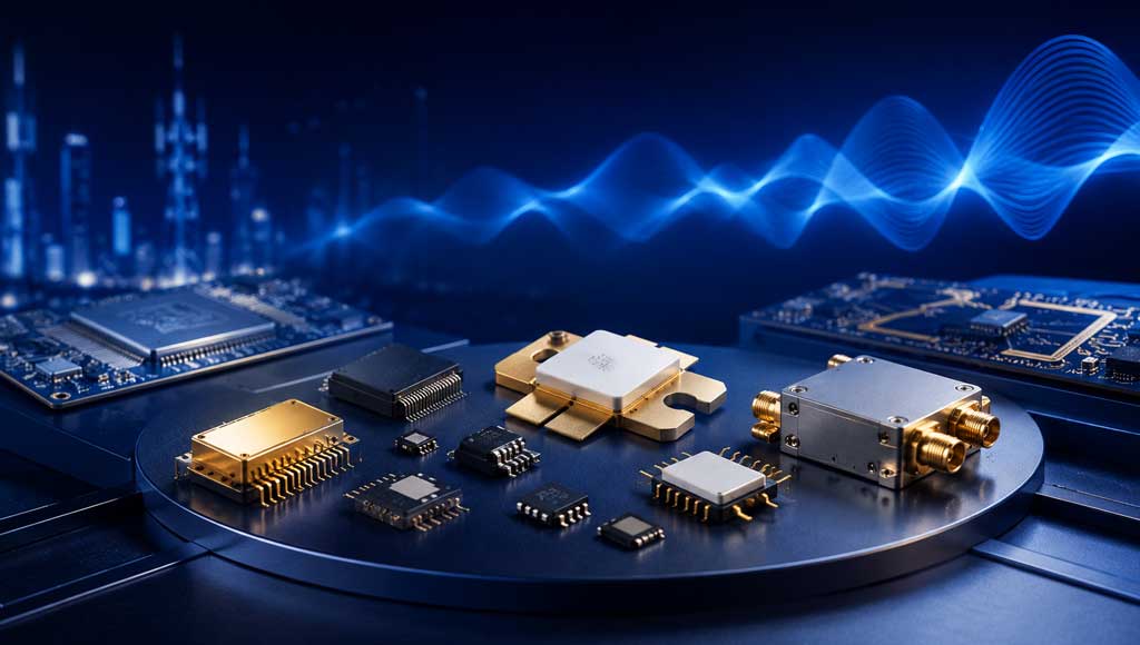
Packaged ICs are standard off-the-shelf components that house RF bare die in plastic or ceramic enclosures, ready for surface-mount assembly on PCBs. Covering frequencies from DC to 40 GHz, they are the most commonly used “plug-and-play” solution for most RF module designs.
GaN Power Devices are high-power, high-efficiency RF amplifiers based on gallium nitride technology, delivering output power up to 100W and covering the 0.5 GHz to 8.0 GHz spectrum. They are the technology of choice for high-power applications such as radar transmitters, electronic warfare systems, and satellite communication uplinks.
STARDL’s product portfolio across both categories – Packaged ICs covering DC to 40 GHz and GaN Power Devices covering 0.5 to 8.0 GHz – provides engineers with a complete RF signal chain solution from receive chain to transmit chain.
1. What Are RF Microwave ICs?
RF microwave ICs are fundamentally different from traditional digital ICs. Digital ICs care about the logical correctness of “0”s and “1”s, while RF ICs care about signal amplitude, phase, frequency, noise, and power – the performance of these analog quantities at GHz frequencies determines the upper limit of the entire system.
RF microwave ICs can be divided into two major categories:
Hybrid Microwave Integrated Circuits: Integrate multiple bare die of different processes and materials (such as GaAs LNA, GaN PA, silicon-based switches) on a ceramic or metal substrate, interconnected through micro-assembly techniques to form a complete RF functional module.
Monolithic Microwave Integrated Circuits (MMIC): Fabricate the entire RF functional circuit on a single semiconductor chip using semiconductor processes. Typical MMIC examples include GaAs HEMT and GaN HEMT implementations of LNAs, PAs, mixers, and more.
2. STARDL’s RF Microwave IC Portfolio
STARDL offers a high-performance RF, microwave, and millimeter-wave integrated circuit portfolio covering frequencies from low GHz through millimeter-wave bands. The portfolio covers complete signal chain functions including signal transmission, amplification, frequency conversion, routing, attenuation, and precision timing control.
Products are organized into three major categories: Matriz nua, Packaged ICs, and GaN Power Devices.
Matriz nua are unpackaged wafer-level chips that eliminate package parasitics for minimal signal loss and excellent thermal dissipation, with frequency capability extending to 50 GHz. These products are suitable for radar front-ends and wideband transceivers where micro-assembly capability exists and ultimate performance is required.
Packaged ICs are ready-to-use standard SMT devices covering DC to 40 GHz, available in both plastic and ceramic packaging options.
GaN Power Devices are high-power, high-efficiency RF front-end components based on gallium nitride technology, delivering output power up to 100W and covering the 0.5 GHz to 8.0 GHz spectrum.
The following sections focus on Packaged ICs and GaN Power Devices.
3. Packaged ICs: Making RF Design Simpler
3.1 What Are Packaged ICs?
Packaged ICs are RF bare die enclosed in plastic or ceramic housings, forming standard components ready for surface-mount (SMT) assembly on PCBs.
Compared to bare die, Packaged ICs offer several advantages:
Lower design barrier. Using bare die requires mastering micro-assembly processes – die attach, wire bonding, eutectic soldering – capabilities that not every R&D team possesses. Packaged ICs with SMT packages are compatible with standard assembly processes and can be handled by any factory with basic SMT capability.
Higher reliability. Ceramic packaging provides hermetic protection, ensuring stable operation in harsh environments including moisture, salt spray, and temperature shock. This is critical for military, aerospace, and outdoor communication equipment.
Simplified supply chain. A single packaged IC replaces the complex “bare die procurement + micro-assembly outsourcing” process, making procurement, inventory, and quality control much simpler.
3.2 STARDL Packaged IC Product Line
STARDL’s Packaged IC product line covers DC to 40 GHz and includes the following categories:
Low-Noise Amplifiers (LNA) – Based on GaAs process, providing extremely low noise figure at the first stage of the receive chain, determining the upper limit of the entire system’s sensitivity. STARDL’s LNAs achieve noise figures as low as 0.35 dB, competitive within this product class.
Broadband Driver Amplifiers and Power Amplifiers – Providing gain and output power drive capability for the signal chain.
High-Isolation Digital RF Switches – Supporting up to SP6T configurations, offering low insertion loss and high isolation in signal routing.
Atenuadores, limitadores e equalizadores – For signal amplitude control and protection.
3.3 Engineering Considerations for Package Selection
The most overlooked issue when selecting packaged ICs is: the package itself introduces additional parasitic parameters.
The S-parameters provided in datasheets are typically measured on a wafer-level probe station – probes contacting the chip pads directly. But on your PCB, package leads, bond wires, and traces introduce additional inductance and capacitance. These parasitics become significant at high frequencies (especially above 10 GHz), altering impedance matching conditions.
STARDL’s packaged IC designs undergo rigorous package co-simulation optimization across the full frequency range, ensuring minimum performance degradation from bare die to packaged device.
4. GaN Power Devices: Redefining High-Power RF
4.1 Why GaN?
Gallium nitride (GaN) is the most representative RF power technology among third-generation semiconductor materials. Compared with traditional GaAs and silicon-based processes, GaN offers three core advantages:
High power density. GaN has a bandgap of 3.4 eV, more than twice that of GaAs (1.4 eV). This means that for the same transistor size, GaN can handle much higher voltage and current density, delivering several times the output power of GaAs.
High efficiency. GaN HEMTs feature low on-resistance and fast switching speed, achieving drain efficiency above 60% in RF power amplification.
High thermal stability. GaN devices exhibit far less performance drift at high temperatures than GaAs devices, making them particularly suitable for high-power, high-temperature applications such as radar transmitters, electronic warfare systems, and satellite communication terminals.
4.2 Market Trends for GaN Power Devices
The global RF GaN market was valued at approximately $1.894 billion in 2025 and is projected to reach $3.536 billion by 2030, at a CAGR of 13.29%. Other research indicates that the global GaN RF chip market has already exceeded $3.42 billion in 2025, growing 27.6% from 2024, and is expected to climb to $9.87 billion by 2030.
Key growth drivers for the RF GaN market include: 5G base station deployment, the proliferation of Active Electronically Scanned Array (AESA) radars, upgrades to satellite communication systems, and modernization of electronic warfare equipment.
4.3 STARDL’s GaN Power Device Product Line
STARDL’s GaN Power Device product line covers the 0.5 GHz to 8.0 GHz frequency band, offering both Continuous Wave (CW) and pulsed operating modes.
Frequency coverage: From L-band (1-2 GHz) through C-band (4-8 GHz), covering the core bands for radar, satellite communications, and infrastructure base stations.
Output power: Up to 61.5 dBm (approximately 141W), meeting high-power requirements from tactical radar to long-range satellite communications.
Operating modes: CW mode for continuous transmission scenarios (such as satellite communication uplinks), pulsed mode for radar detection scenarios.
Product forms: Including internally-matched power amplifiers (Internally-Matched PA) with built-in pre-matched impedance networks that simplify external matching circuit design.
STARDL’s GaN power devices feature pre-matched internal impedance networks that maintain stable linearity and ruggedness under large-signal, CW, or pulsed operating modes.
5. Selection Decision: Packaged ICs vs. GaN Power Devices
| Dimensão | Packaged ICs | GaN Power Devices |
|---|---|---|
| Aplicações típicas | Low-to-medium power signal chains, receive chains, general RF modules | High-power transmit chains, radar front-ends, SATCOM uplinks |
| Gama de frequências | DC – 40 GHz | 0.5 – 8.0 GHz |
| Output Power | Milliwatts to a few watts | Up to 100W+ |
| Package Type | SMT plastic/ceramic | Internally-matched modules/ceramic |
| Design Complexity | Low (standard SMT assembly) | High (requires bias, thermal management) |
| Common Use Cases | Receiver LNAs, RF switches, driver amps | Radar PAs, EW systems, SATCOM terminals |
When making a selection decision, consider these three dimensions:
Power requirements. If you need milliwatts to a few watts of output power, Packaged ICs are the simpler, more economical choice. If you need tens or even hundreds of watts of transmit power – such as for radar transmitters or satellite communication uplinks – GaN Power Devices are unavoidable.
Design capability. Packaged ICs have lower design requirements – standard SMT processes combined with datasheet guidance are sufficient. GaN Power Devices require deeper RF design expertise – bias circuit design, thermal management, pulse modulation matching – all of which directly affect whether the device can achieve datasheet performance.
Environmental requirements. If the system must operate reliably for extended periods in harsh environments with high temperature, humidity, or vibration, ceramic-packaged GaN devices offer a clear reliability advantage.
6. STARDL’s Engineering Advantages
STARDL’s core strengths in RF microwave ICs are evident across three dimensions:
Full-chain coverage. From low-noise amplifiers to power amplifiers, from mixers to switches, from bare die to packaged devices, STARDL provides a complete RF signal chain solution. This means engineers can source all core devices for both receive and transmit chains from a single supplier, eliminating multi-vendor coordination issues.
Comprehensive frequency coverage. From DC through 50 GHz, covering all mainstream applications including radar, satellite communications, and 5G infrastructure.
Engineering-driven design. STARDL’s products are designed not just for lab performance, but for stability and reliability in real-world system environments. Products are optimized for high-density system integration, helping engineering teams simplify RF front-end design, optimize thermal management, and overcome space constraints.
A Realidade da Engenharia
RF microwave integrated circuits are the foundational building blocks of radar, satellite communications, and wireless systems. Understanding the characteristics and applicable scenarios of Packaged ICs and GaN Power Devices is the first step toward successful RF front-end design.
For teams pursuing design efficiency and rapid production, Packaged ICs provide a mature “ready-to-use” solution. For teams pursuing ultimate power output and high-performance in radar transmitters or satellite communication uplinks, GaN Power Devices offer the optimal combination of power density and efficiency available today.
STARDL’s product portfolio across both directions – Packaged ICs covering DC to 40 GHz and GaN Power Devices covering 0.5 to 8.0 GHz with output up to 100W – provides engineers with complete options for diverse application needs.
Interested in STARDL’s RF microwave IC products? Visit stardl.com/rf-microwave-ics/ for detailed technical documentation and product datasheets.